|
|
Pixie
2 Transceiver
|

IntroductionThe Pixie 2 is a tiny radio transceiver, suitable for sending and receiving Morse code. It can be operated on the 80m (3.5MHz) and 40m (7MHz) amateur radio bands by choosing a suitable crystal. The original circuit was designed by Dave Joseph, W7AMX based on the earlier Micro-80 mini-transceiver by Oleg Borodin, RV3GM. Doug Hendricks, KI6DS drew a schematic and designed the original PCB layout for the Pixie 2 transceiver. The Pixie 2 first appeared in the June 1995 issue of the NorCal QRP Club's magazine called "QRPp". Additional information on the history of the Pixie 2 transceiver can be found at the QRPp International website. |
ModificationsThe simplicity of the design has encouraged experimentation, with the result that there are many variations on the original circuit in existence today. The version presented below adds a trimming capacitor and makes a number of component changes to the original design. ConstructionThe revised circuit required layout of a new Printed Circuit Board (PCB). The transceiver was constructed on this board and successfully tested. |
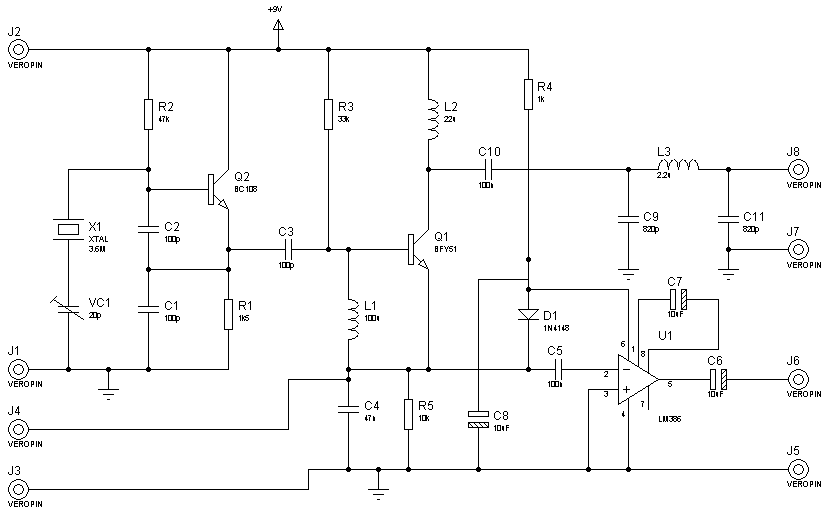
Circuit DiagramThe Pixie 2 consists of a Colpitts oscillator, a power amplifier/mixer and an audio amplifier. Power is supplied from a 9V battery to vero-pins J1 and J2, while a Morse key is connected between J3 and J4. A pair of headphones is connected to J5 & J6. To operate successfully, the transceiver must be grounded at pin J7 and an antenna consisting of a long length of wire connected to J8. The continuously running oscillator consists of transistor Q2, crystal X1 and the surrounding passive components. The frequency of oscillation can be varied from the crystal's fundamental frequency by a few kilohertz by means of trimmer capacitor VC1. The oscillator output is taken via capacitor C3 to the power/amplifier/mixer circuit. Running the oscillator continuously allows the oscillator to run at a stable frequency, so that the transmitted tone on key-down is clean without the "chirp" that is often heard when the oscillator stage is keyed. The oscillator should be screened so as to minimise unwanted radiation during receive. The Pixie II can operate over a wide range of RF frequencies. Changing the crystal and altering the output filter are the only modifications required. |
During transmit, the Morse key grounds the emitter of Q1, allowing it to function as a Class C power amplifier. This produces harmonics of the fundamental frequency, which are attenuated by the low-pass filter comprising C9, L3 & C11. Further attenuation can be achieved by connecting the transceiver to the antenna via an Antenna Tuning Unit (ATU), which will also improve the impedance matching. Lastly the audio amplifier U1 is disabled during transmit, by removing it's power via D1 when the Morse key is down. During receive, transistor Q1 operates as a mixer. The received signal enters via the collector, whilst the local oscillator (Q2) signal is applied to the base. The frequency difference signal emerges from Q1's emitter and is amplified by audio amplifier U1. An audio tone is heard provided the received signal is slightly off-frequency compared to the transmit frequency being produced by the local oscillator. If the received signal is at exactly the same frequency as the transmit frequency, it is necessary to adjust trimmer VC1 until a tone is heard. Trimmer VC1 should be returned to the previous position when transmitting. |
 |
|
Bill of MaterialsDesign: C:\User\proteus\Pixie2.DSN
Doc. no.: <NONE>
Revision: <NONE>
Author: <NONE>
Created: 10/01/03
Modified: 14/01/03
Partslist generated OK.
QTY PART-REFS VALUE
--- --------- -----
Resistors
---------
1 R1 1k5
1 R2 47k
1 R3 33k
1 R4 1k
1 R5 10k
Capacitors
----------
3 C1,C2,C3 100p
1 C4 47n
2 C5,C10 100n
3 C6,C7,C8 10uF
2 C9,C11 820p
Integrated Circuits
-------------------
1 U1 LM386
Transistors
-----------
1 Q1 BFY51
1 Q2 BC108
Diodes
------
1 D1 1N4148
Miscellaneous
-------------
8 J1,J2,J3,J4,J5,J6,J7,J8 VEROPIN
1 L1 100u
1 L2 22u
1 L3 2.2u
1 VC1 20p
1 X1 XTAL
|
|
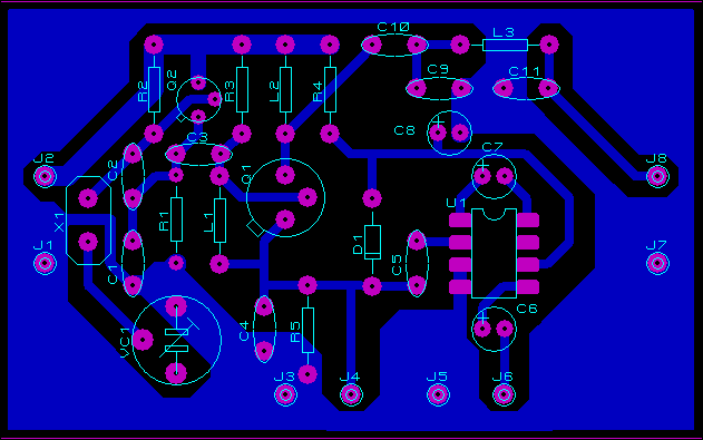
Component LayoutThis is the view from the top of the board. Mounting holes (not shown) can be drilled in the four corners.
|
|
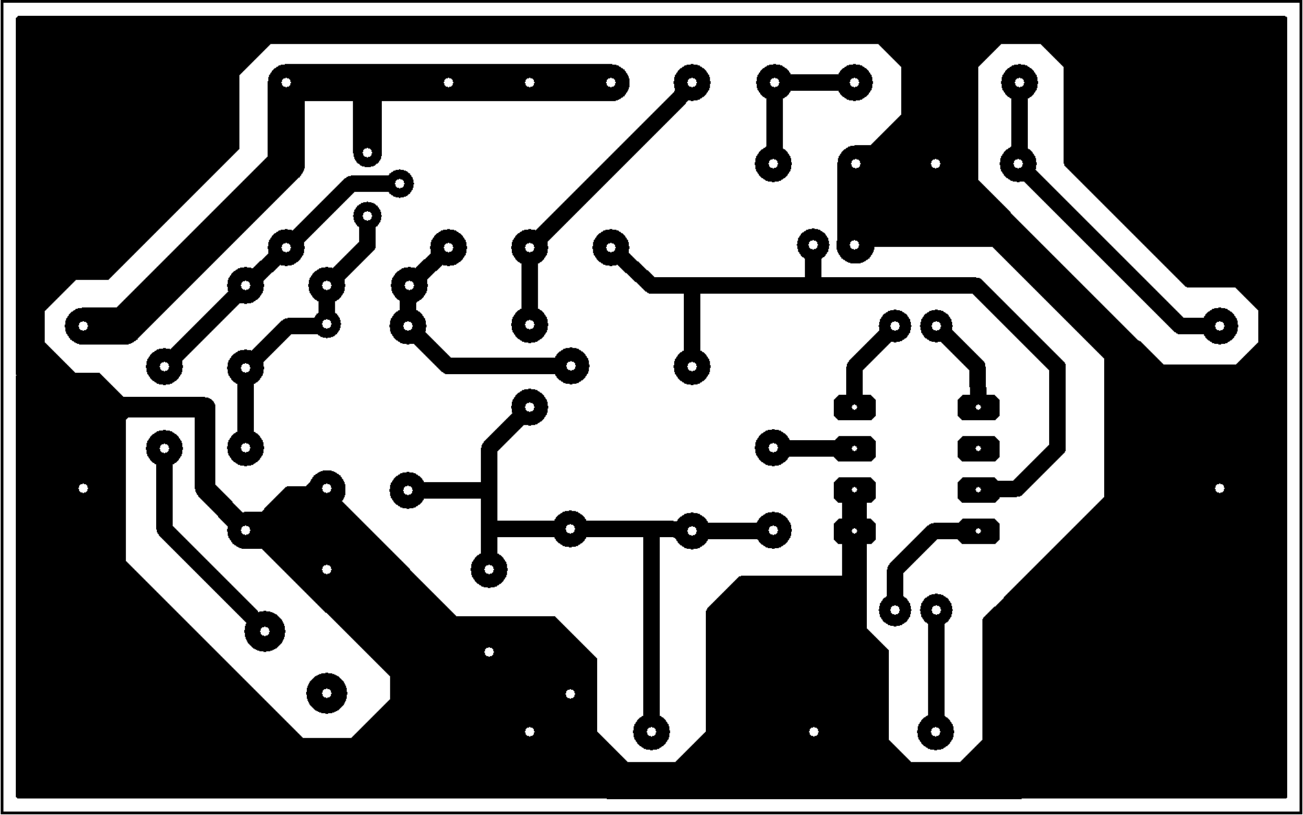
Printed Circuit Board ArtworkThis is the view from the top of the board. Click on the image for a high resolution version.
|
|